Wafer Defect Detection using Vision Transformers
Overview
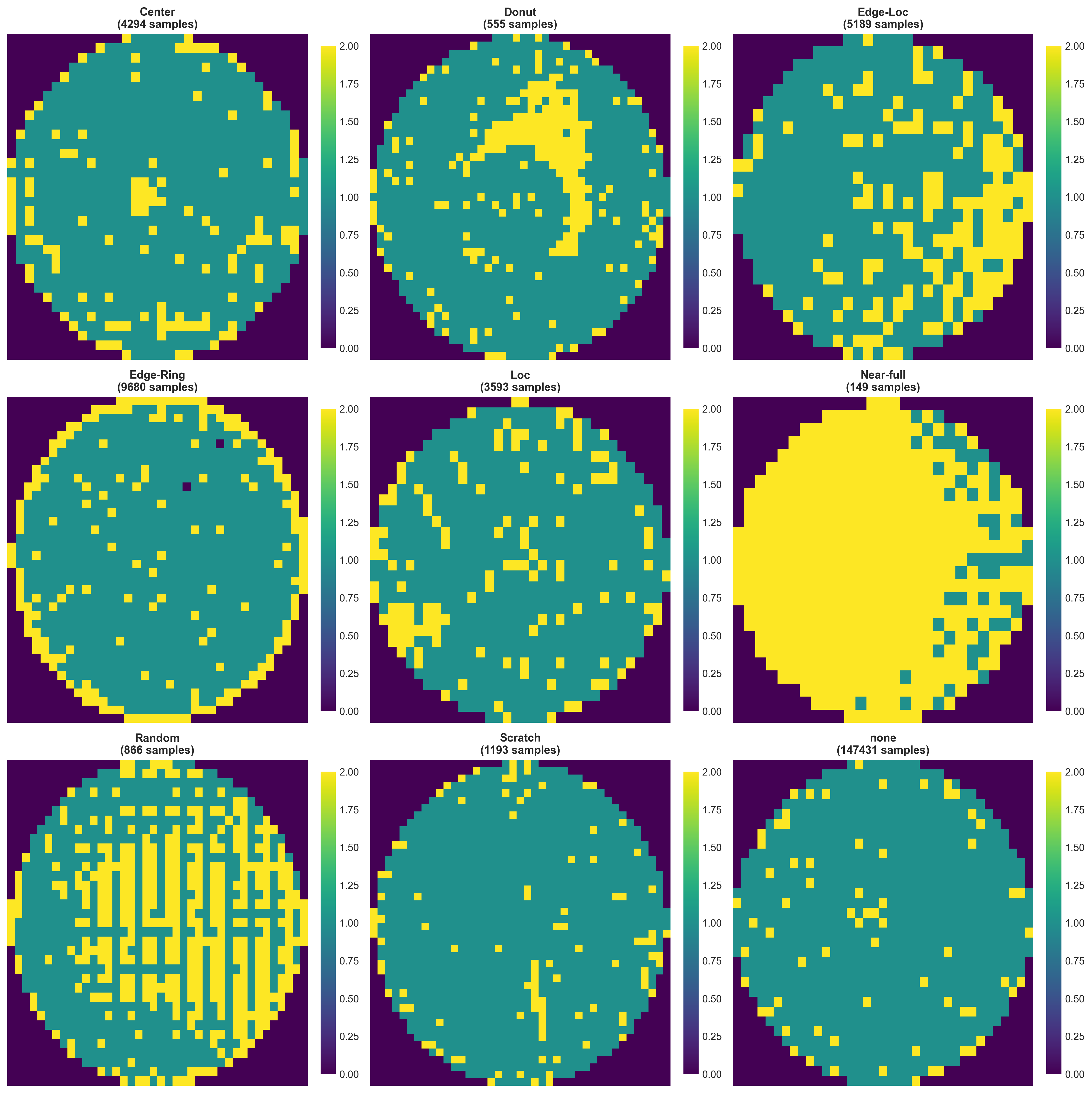
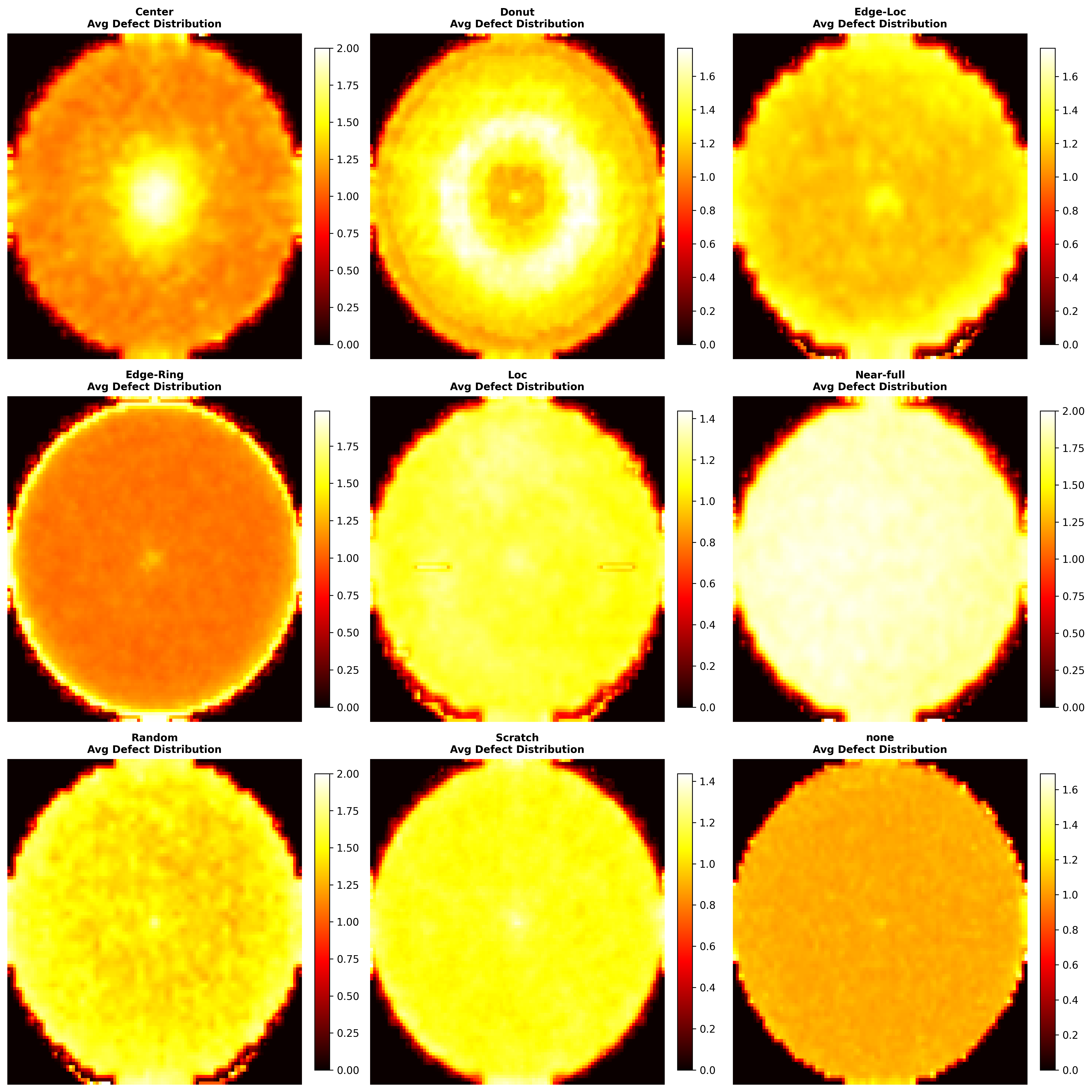
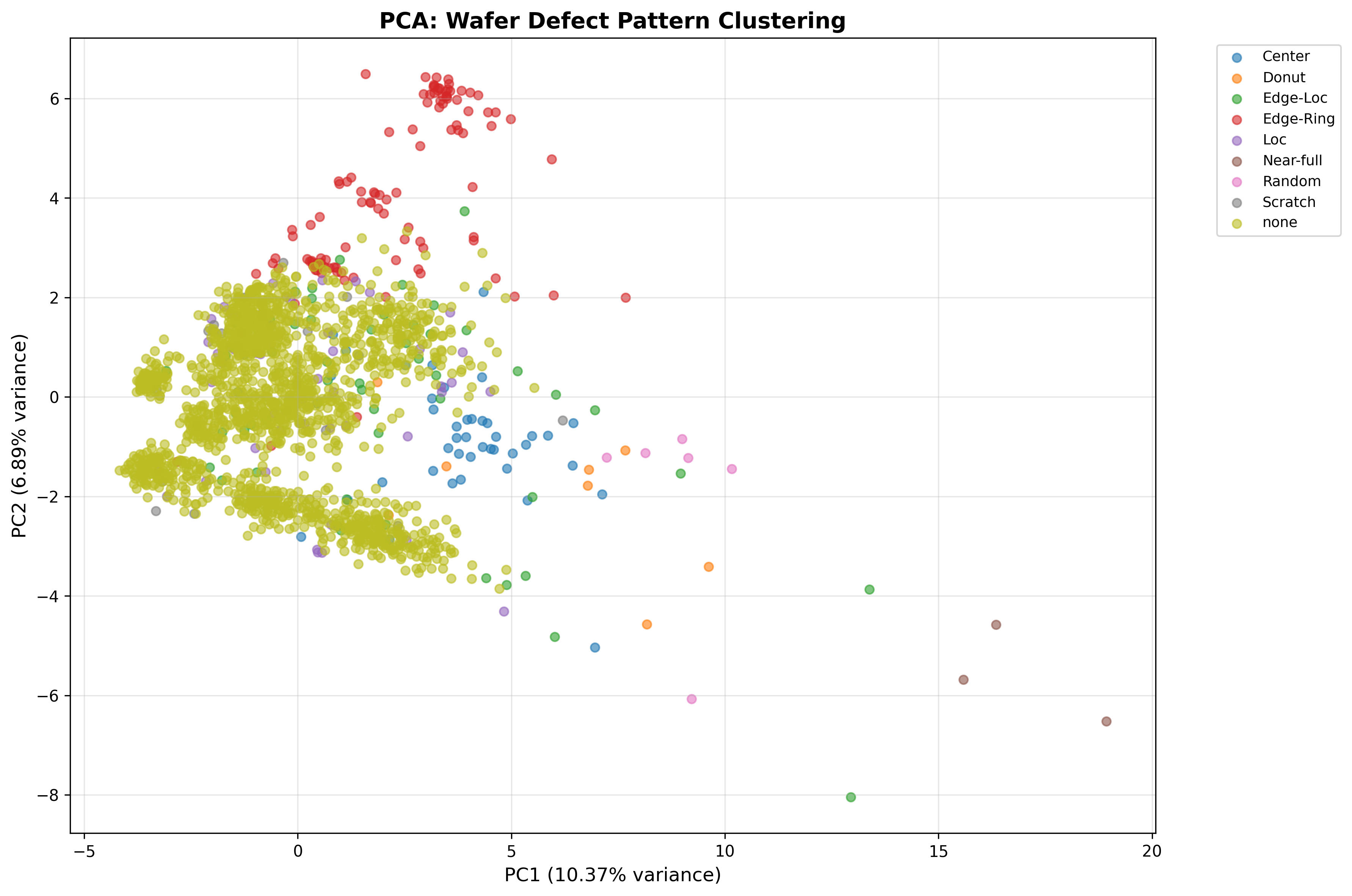
Developed a Vision Transformer (ViT-tiny) classification system for detecting and categorizing defect patterns on semiconductor wafers. Using the WM-811K dataset containing over 170,000 labeled wafer maps from real manufacturing processes, the model learns to identify 9 distinct defect patterns including Center, Donut, Edge-Ring, Scratch, and Random defects that occur during semiconductor fabrication.
Problem Statement
Semiconductor manufacturers face significant challenges in identifying defect patterns on wafers during fabrication. Manual inspection is slow, error-prone, and cannot handle the scale of modern production. Existing automated systems lack the accuracy needed for production deployment, and the severe class imbalance (85% normal wafers) makes it difficult to detect rare but critical defect patterns.
Approach
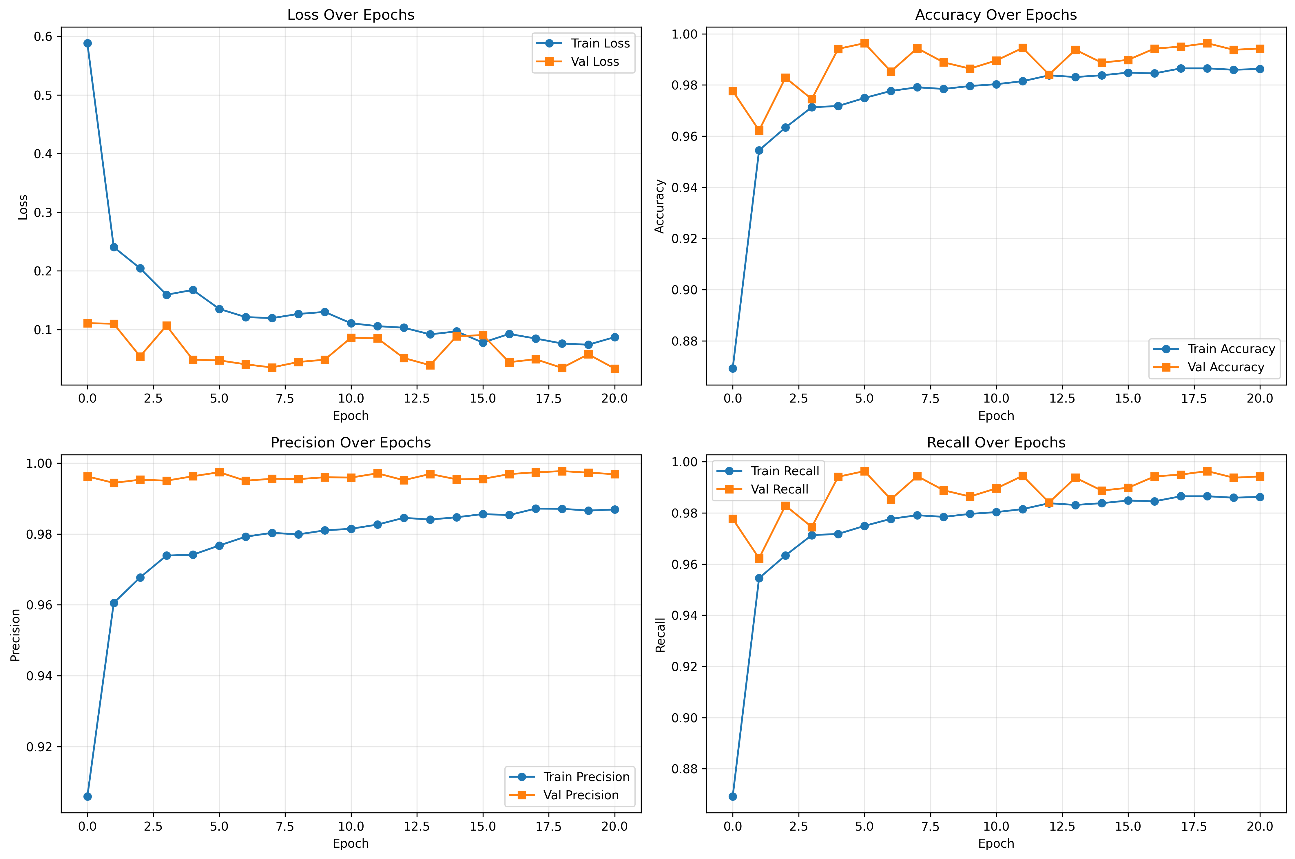
Implemented a Vision Transformer (ViT-tiny) architecture with pretrained ImageNet weights for transfer learning. Used mixed precision training (FP16) for faster convergence, class-weighted loss functions to handle severe imbalance, and comprehensive data augmentation (rotation, flips, color jitter). The model processes 224x224 wafer maps through 12 transformer layers with multi-head self-attention, enabling it to learn spatial defect patterns. Training utilized AdamW optimizer with cosine annealing and early stopping for optimal convergence.
Visualizations
Results
Achieved exceptional performance with 99.63% test accuracy on 118,595 wafer samples, surpassing the target range of 85-95%. The model demonstrated 99%+ weighted F1-score across all 9 defect classes, even on minority classes with limited samples. Converged in just 6 epochs (~3 hours on A100 GPU) with stable training and no overfitting. The lightweight model (21MB, 5.5M parameters) enables fast inference (<10ms per image), making it production-ready for real-time quality control in semiconductor fabs.